Digital Circuit Design with FPGAs: Core Concepts - kapak
Teknoloji#fpga#digital design#logic elements#lut

Digital Circuit Design with FPGAs: Core Concepts

Explore the fundamental components and design flow of digital circuits using FPGAs, including Logic Elements, Look-Up Tables, and state machine implementation.

lqyarxg2January 25, 2026 ~20 dk toplam
01

Sesli Özet

6 dakika

Konuyu otobüste, koşarken, yolda dinleyerek öğren.

Sesli Özet

Digital Circuit Design with FPGAs: Core Concepts

0:006:15
02

Flash Kartlar

25 kart

Karta tıklayarak çevir. ← → ile gez, ⎵ ile çevir.

1 / 25
Tüm kartları metin olarak gör
  1. 1. What is the primary focus of this content regarding digital circuit design?

    The content primarily focuses on digital circuit design as implemented within Field-Programmable Gate Arrays (FPGAs). It aims to provide foundational elements and operational principles, guiding through core components and how intricate systems are constructed and configured in FPGAs.

  2. 2. What does the acronym FPGA stand for, and what is its significance in hardware implementation?

    FPGA stands for Field-Programmable Gate Array. Its significance lies in offering immense flexibility and power in hardware implementation, allowing designers to configure and reconfigure digital circuits in the field after manufacturing, adapting to various application needs.

  3. 3. What are the essential building blocks that allow FPGAs to offer flexibility and power?

    The essential building blocks explored range from basic logic gates to complex state machines. These fundamental components, such as Look-Up Tables (LUTs), Registers (Flip-Flops), and Multiplexers, are crucial for constructing the intricate digital logic within an FPGA.

  4. 4. Describe the function of a 4-input Look-Up Table (LUT) in an FPGA.

    A 4-input Look-Up Table (LUT) is a fundamental logic element in an FPGA that acts as a truth table. It defines the output for every possible combination of its inputs, effectively implementing a specific Boolean function. Its output can be purely combinational or synchronized with a clock signal.

  5. 5. What are the two main types of output a LUT can provide, and what is the difference?

    A LUT can provide either a purely combinational output or an output synchronized with a clock signal. A combinational output changes immediately with its inputs, while a synchronized output provides a stable, timed output, typically at the edge of a clock pulse, which is essential for sequential logic.

  6. 6. What is a 1-bit Register often implemented as, and why is it vital for digital circuits?

    A 1-bit Register is often implemented as a Flip-Flop. It is vital for digital circuits because it stores state information, allowing the circuit to 'remember' past inputs or conditions. This capability is fundamental for building sequential logic, where the output depends not only on current inputs but also on the history of inputs.

  7. 7. Explain the role of Multiplexers within an FPGA architecture.

    Multiplexers play a critical role in FPGAs as data selectors. They are designed to choose one of several input signals and then forward the selected input onto a single output line. This functionality is essential for routing data and control signals efficiently within the reconfigurable fabric of an FPGA.

  8. 8. Name the three fundamental logic elements that form the basic toolkit for constructing complex digital logic within an FPGA.

    The three fundamental logic elements that form the basic toolkit for constructing complex digital logic within an FPGA are Look-Up Tables (LUTs), Registers (often implemented as Flip-Flops), and Multiplexers. These components work together to implement both combinational and sequential logic functions.

  9. 9. What is a Logic Array Block (LAB) in the context of a Cyclone IV device?

    In a Cyclone IV device, a Logic Array Block (LAB) is a larger structural unit that groups together multiple smaller logic resources. It typically contains 16 Logic Elements (LEs), along with associated routing and control logic. LABs are key organizational units within the FPGA's programmable fabric.

  10. 10. How many Logic Elements (LEs) does a Logic Array Block (LAB) typically contain in a Cyclone IV device?

    A Logic Array Block (LAB) in a Cyclone IV device typically contains 16 Logic Elements (LEs). These LEs are the smallest configurable units that can implement a piece of logic, and their grouping into LABs helps organize the FPGA's architecture for efficient design and routing.

  11. 11. What is a Logic Element (LE) in an FPGA?

    A Logic Element (LE) is a configurable unit within an FPGA that can implement a small piece of logic. Each LE typically includes a Look-Up Table (LUT) for combinational logic, a Flip-Flop for sequential logic, and a multiplexer for output selection. LEs are the fundamental building blocks for implementing user-defined functions.

  12. 12. Where is the configuration data for Logic Elements (LEs) and their interconnections stored within an FPGA?

    The configuration data that defines the function of Logic Elements (LEs) and their interconnections is held in Static Random-Access Memory (SRAM) within the FPGA. This SRAM stores the bitstream that programs the FPGA's logic and routing paths, making it reconfigurable.

  13. 13. When is the SRAM loaded in an FPGA, and what does this process enable?

    The SRAM in an FPGA is loaded during the device's power-up sequence. This process enables the FPGA to be 'programmable' in the field, meaning its functionality can be defined or redefined after manufacturing by loading new configuration data into its SRAM.

  14. 14. How can a Logic Element (LE) be configured to implement functions, specifically regarding the number of inputs?

    An LE can be configured to implement two independent 4-input functions, often designated as X and Y. Each of these functions typically uses one LE, constrained by area and timing considerations. This allows for efficient utilization of the LE's internal LUTs for smaller logic blocks.

  15. 15. How does an FPGA architecture handle functions that require more than four inputs?

    When dealing with functions that have more than four inputs, the FPGA architecture handles this by cascading multiple LEs or by utilizing specialized routing. This breaks down the larger function into smaller, 4-input segments that individual LUTs within the LEs can manage, effectively implementing complex logic.

  16. 16. What is the first step a designer takes in the overall FPGA configuration process?

    The first step in the overall FPGA configuration process is for a designer to write Hardware Description Language (HDL) code. This is typically done using languages like VHDL or Verilog, which describe the desired digital circuit's behavior at an abstract level.

  17. 17. What is the purpose of Hardware Description Language (HDL) code in FPGA design?

    The purpose of Hardware Description Language (HDL) code, such as VHDL or Verilog, in FPGA design is to describe the desired digital circuit's behavior. It allows designers to specify the logic and interconnections of a circuit in a textual format, which can then be translated into a physical implementation.

  18. 18. What is the next step in the FPGA design flow after writing HDL code?

    The next step in the FPGA design flow after writing HDL code is synthesis. During synthesis, the HDL code is translated into a gate-level netlist, which is then mapped onto the specific physical resources available within the target FPGA device, such as LUTs, Flip-Flops, and routing paths.

  19. 19. Describe what happens during the synthesis stage of the FPGA design flow.

    During the synthesis stage, the Hardware Description Language (HDL) code is translated and mapped onto the specific physical resources of the FPGA. This involves converting the behavioral description into a structural representation using the FPGA's available components like Look-Up Tables (LUTs), Flip-Flops, and routing paths, optimizing for area and timing.

  20. 20. What happens after the synthesis stage in the FPGA design flow?

    After the synthesis stage, the configuration data, also known as the bitstream, is generated. This data is then downloaded to the FPGA's Static Random-Access Memory (SRAM). This step effectively programs the FPGA, configuring its internal logic and routing to implement the designed circuit.

  21. 21. What is the final step in the FPGA design flow, once configuration data is downloaded?

    The final step in the FPGA design flow, once the configuration data is downloaded, is for the FPGA to execute the implemented hardware. At this point, the FPGA performs the functions defined by the designer's code, acting as a custom digital circuit.

  22. 22. How do FPGAs implement sequential logic, particularly state machines, using Logic Elements (LEs)?

    FPGAs implement sequential logic, such as state machines, by chaining Logic Elements (LEs). One LE might compute an intermediate function, and another LE would use its output as an input, creating a logical sequence. The integrated flip-flops within each LE are crucial for holding state bits and preserving the current state until the next clock edge.

  23. 23. How many Logic Elements (LEs) are typically used to generate the next-state logic in a state machine, and what is the role of their integrated flip-flops?

    Typically, two Logic Elements (LEs) are used to generate the next-state logic in a state machine, with one LE dedicated to each state bit. Each LE's integrated flip-flop is crucial as it holds one state bit, preserving the current state of the machine until the next clock edge, which is fundamental for sequential operation.

  24. 24. How are critical control signals like reset, load, and enable managed within an LE in an FPGA?

    Critical control signals such as reset, load, and enable are not handled externally by the designer's logic directly but are managed by the internal LE control logic. This simplifies the design process for the user and ensures proper synchronization and reliable operation of the flip-flops within the Logic Elements.

  25. 25. Define what a Decoder is in the context of digital circuit components, providing an example.

    A Decoder is a digital circuit component that takes a set of binary inputs and activates one of several outputs based on the binary value of those inputs. For example, a 2:4 decoder takes two inputs (say, A and B) and activates one of four unique output lines corresponding to the binary combinations of A and B.

03

Bilgini Test Et

15 soru

Çoktan seçmeli sorularla öğrendiklerini ölç. Cevap + açıklama.

Soru 1 / 15Skor: 0

What is the primary function of a Look-Up Table (LUT) in an FPGA?

04

Detaylı Özet

4 dk okuma

Tüm konuyu derinlemesine, başlık başlık.

This study material has been compiled from a lecture audio transcript and a PDF document, providing a comprehensive overview of digital circuit design with FPGAs.


📚 Digital Circuit Design with FPGAs: A Study Guide

🚀 Introduction to FPGAs and Digital Design Fundamentals

Field-Programmable Gate Arrays (FPGAs) are powerful, reconfigurable integrated circuits that allow designers to implement custom digital logic. Understanding their core components and operational principles is crucial for modern digital design. This guide explores the essential building blocks and design flow that enable FPGAs to offer immense flexibility and power in hardware implementation, from basic logic elements to complex state machines.

⚙️ Fundamental Logic Elements in FPGAs

At the heart of FPGA functionality are several key logic elements that serve as the basic toolkit for constructing complex digital logic.

1️⃣ Look-Up Table (LUT)

📚 Definition: A Look-Up Table (LUT) is a fundamental component in FPGAs, essentially acting as a truth table. ✅ Functionality: * It defines the output for every possible combination of its inputs. * In an FPGA, a LUT shows the specific inputs and outputs for the logic it implements. * Commonly, FPGAs use 4-input LUTs. ✅ Output Types: * Combinational: The output changes immediately with its inputs. * Synchronized: The output is stable and timed, often with a clock signal. 💡 Insight: LUTs are highly flexible, capable of implementing any Boolean function up to their input capacity.

2️⃣ 1-bit Register (Flip-Flop)

📚 Definition: A 1-bit Register, often implemented as a Flip-Flop, is a sequential logic element. ✅ Functionality: * It is vital for storing state information. * Allows digital circuits to "remember" past inputs or conditions. * Fundamental for sequential logic, where the output depends not only on current inputs but also on past inputs.

3️⃣ Multiplexers (Muxes)

📚 Definition: Multiplexers are data selectors. ✅ Functionality: * They choose one of several input signals. * They forward the selected input onto a single output line. * Crucial for routing data and selecting specific logic paths within the FPGA.

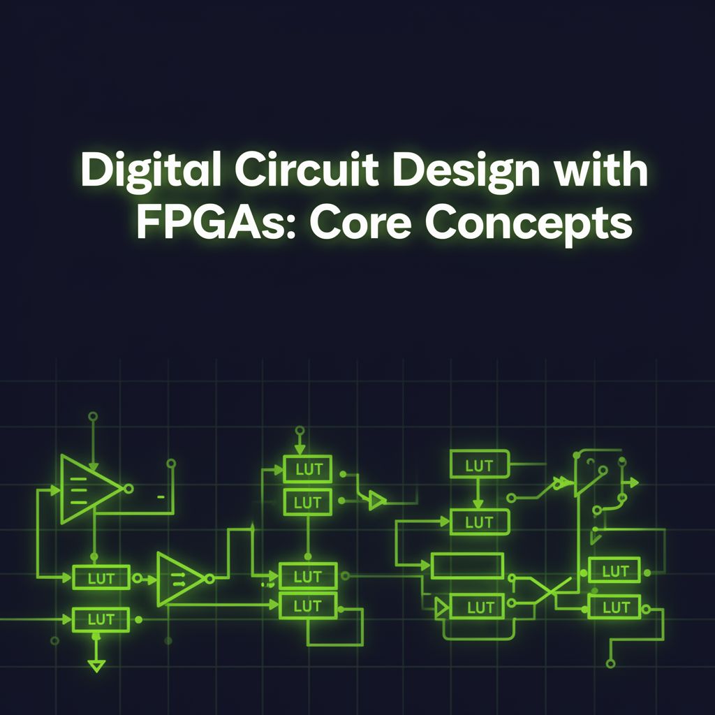
🏗️ FPGA Architecture and Logic Elements (Example: Cyclone IV)

Let's explore how these fundamental elements are integrated within an FPGA architecture, using the Cyclone IV as an example.

Logic Array Block (LAB)

Structure: A Logic Array Block (LAB) is a larger organizational unit within an FPGA. * In a Cyclone IV device, a LAB typically contains 16 Logic Elements (LEs).

Logic Element (LE)

📚 Definition: A Logic Element (LE) is the smallest configurable unit within an FPGA that can implement a piece of logic. ✅ Configuration: * The configuration data defining the function of LEs and their interconnections is held in Static Random-Access Memory (SRAM) within the FPGA. * This SRAM is loaded during the FPGA's power-up sequence, making the device "programmable" in the field. ✅ Functionality: * An LE can be configured to implement two independent 4-input functions, often designated as X and Y. * Each function typically uses one LE, constrained by area and timing. * Example: Inputs like data1 and data3 might connect to variables, while data4 could be tied to a constant value like '0'. * Final multiplexers within the LE select the appropriate LUT outputs to form the desired logic. ✅ Handling Complex Functions: * For functions with more than four inputs (e.g., x = KLM), the FPGA handles this by: * Cascading multiple LEs. * Utilizing specialized routing to break down the larger function into smaller, 4-input segments that individual LUTs can manage.

📊 FPGA Design Flow: From Code to Hardware

The process of designing and implementing a digital circuit on an FPGA follows a structured flow:

  1. ✍️ Hardware Description Language (HDL) Design:
    • The designer writes HDL code (typically VHDL or Verilog).
    • This code describes the desired digital circuit's behavior.
  2. ⚙️ Synthesis:
    • The HDL code is translated and mapped onto the specific physical resources of the FPGA.
    • This includes mapping logic to LUTs, Flip-Flops (FFs), and routing paths.
  3. ⬇️ Configuration Data Download:
    • Once synthesized, the configuration data is generated.
    • This data is then downloaded to the FPGA's internal SRAM.
  4. 🚀 Hardware Execution:
    • The FPGA executes the implemented hardware, performing the functions defined by the designer's code.

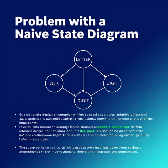
🔄 Implementing Sequential Logic and State Machines

FPGAs are highly adept at implementing sequential logic, particularly finite state machines (FSMs).

State Machine Implementation: * Intermediate Functions: One LE (e.g., LE1) might compute an intermediate function. * Chaining Logic: Another LE (e.g., LE2) would then use LE1's output as one of its own inputs, creating a chain of logic for complex state transitions. * Next-State Logic: Typically, two LEs are used to generate the next-state logic. * State Bit Storage: Each LE's integrated flip-flop holds one state bit, preserving the current state until the next clock edge. * Internal Control: Critical control signals (reset, load, enable) are managed by the internal LE control logic, simplifying the design process and ensuring proper synchronization.

➕ Other Relevant Digital Concepts

Beyond the core FPGA components, other digital circuit concepts are important:

  • Decoders:
    • Function: A decoder takes n inputs and activates one of 2^n outputs based on the binary value of the inputs.
    • Example: A 2:4 decoder takes two inputs (A, B) and activates one of four outputs.
  • Programmable Logic Arrays (PLAs):
    • Function: PLAs are another type of programmable logic device.
    • They are capable of implementing sum-of-products logic forms, offering flexibility in realizing Boolean functions.
  • Pseudo-nMOS Circuits: This refers to a specific circuit style, often used in older or specialized digital designs, which falls under the broader umbrella of digital design techniques.

This guide provides a foundational understanding of FPGA architecture, design flow, and key digital logic concepts, essential for anyone studying modern digital hardware implementation.

Kendi çalışma materyalini oluştur

PDF, YouTube videosu veya herhangi bir konuyu dakikalar içinde podcast, özet, flash kart ve quiz'e dönüştür. 1.000.000+ kullanıcı tercih ediyor.

Sıradaki Konular

Tümünü keşfet
Programming Language Data Types and Memory Management

Programming Language Data Types and Memory Management

An in-depth look into record types, tuples, unions, pointers, references, heap allocation, garbage collection, and type checking in programming languages.

Özet 25 15
Understanding Data Types in Programming Languages

Understanding Data Types in Programming Languages

Explore the fundamental concepts of data types, including primitive types, character strings, arrays, and associative arrays, and their implementation in programming.

Özet 25 15
Syntax Analysis and Parsing Techniques in Language Implementation

Syntax Analysis and Parsing Techniques in Language Implementation

Explore the core concepts of syntax analysis, lexical analysis, and different parsing approaches, including LL and the powerful LR shift-reduce parsers.

Özet 25 15
A Brief History of Programming Languages

A Brief History of Programming Languages

Explore the evolution of programming languages from early pioneers and low-level systems to modern high-level and object-oriented paradigms, covering key innovations and their impact.

Özet 25 15
Names, Bindings, and Scopes in Programming Languages

Names, Bindings, and Scopes in Programming Languages

Explore fundamental concepts of names, variables, binding, scope, and named constants in programming languages, crucial for understanding program execution and design.

Özet 25 15
Syntax Analysis and Parsing Techniques

Syntax Analysis and Parsing Techniques

Explore the fundamentals of syntax analysis, lexical analysis, and different parsing approaches, including LL and the widely used LR parsers.

Özet 25 15
Compiler Design: Lexical Analysis and Parsing Techniques

Compiler Design: Lexical Analysis and Parsing Techniques

Explore the challenges of naive state diagrams in lexical analysis, simplification techniques like character classes, and the fundamental concepts of parsing, including top-down and bottom-up approaches, left recursion, and predictive parsing.

Özet 25 15
Lexical and Syntax Analysis in Language Processors

Lexical and Syntax Analysis in Language Processors

Explore the fundamental stages of language implementation: lexical analysis (scanning) and syntax analysis (parsing), their roles, and theoretical underpinnings.

Özet 25 15